3D Printed PCBA Test Fixtures
I recently released Rev 4 of my USB-C PD Breakout Board. One of the changes from Rev 3 is better DFM, namely adding testpoints for future fixtures. Testing the Rev 3 boards 100 at a time by manually plugging in jumpers was getting old. Once I had the PCB design locked down and sent for fab, I turned my attention towards prototyping the test fixture. Here are some thoughts and documentation of my process of designing and testing the fixture.
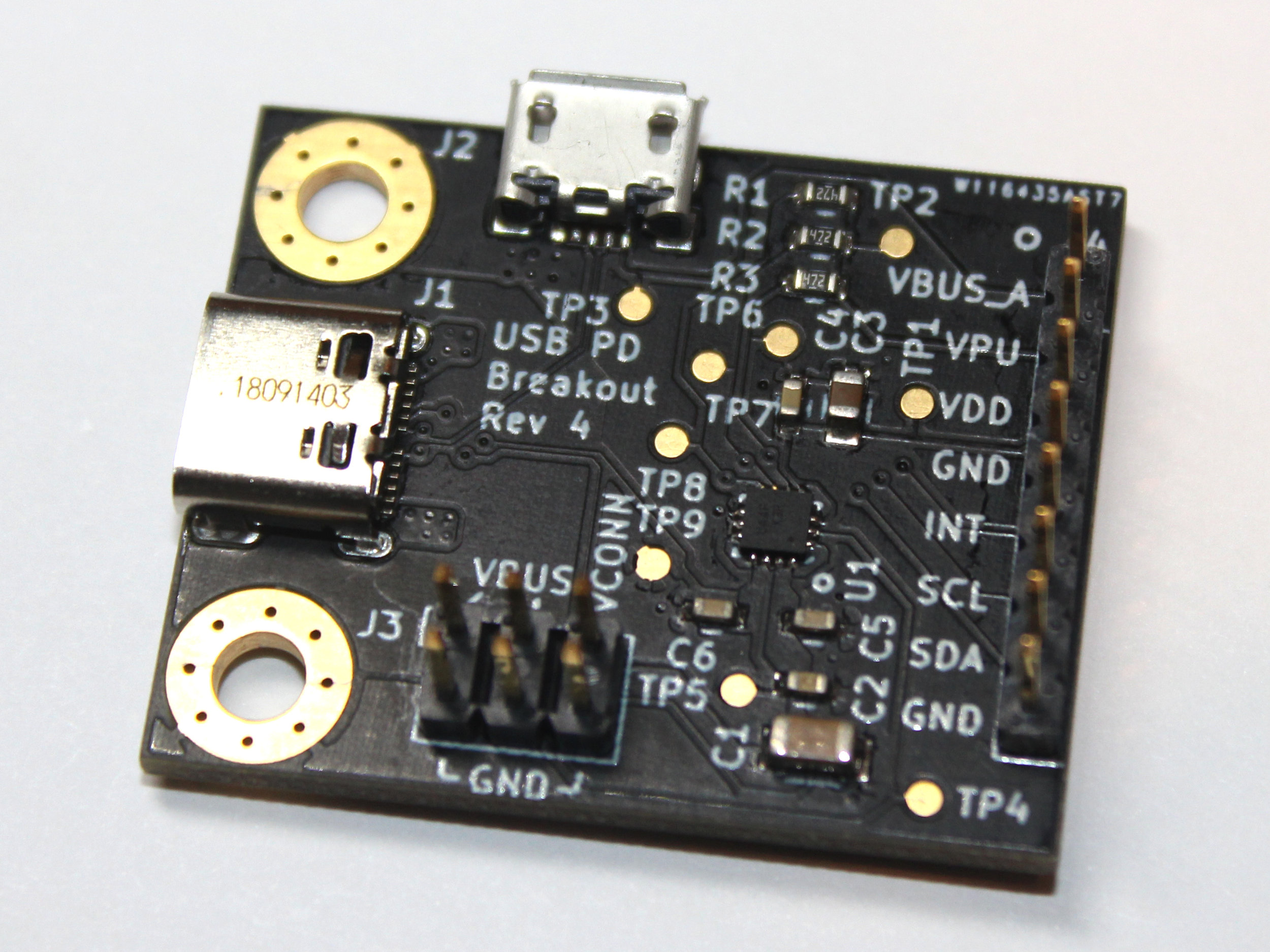
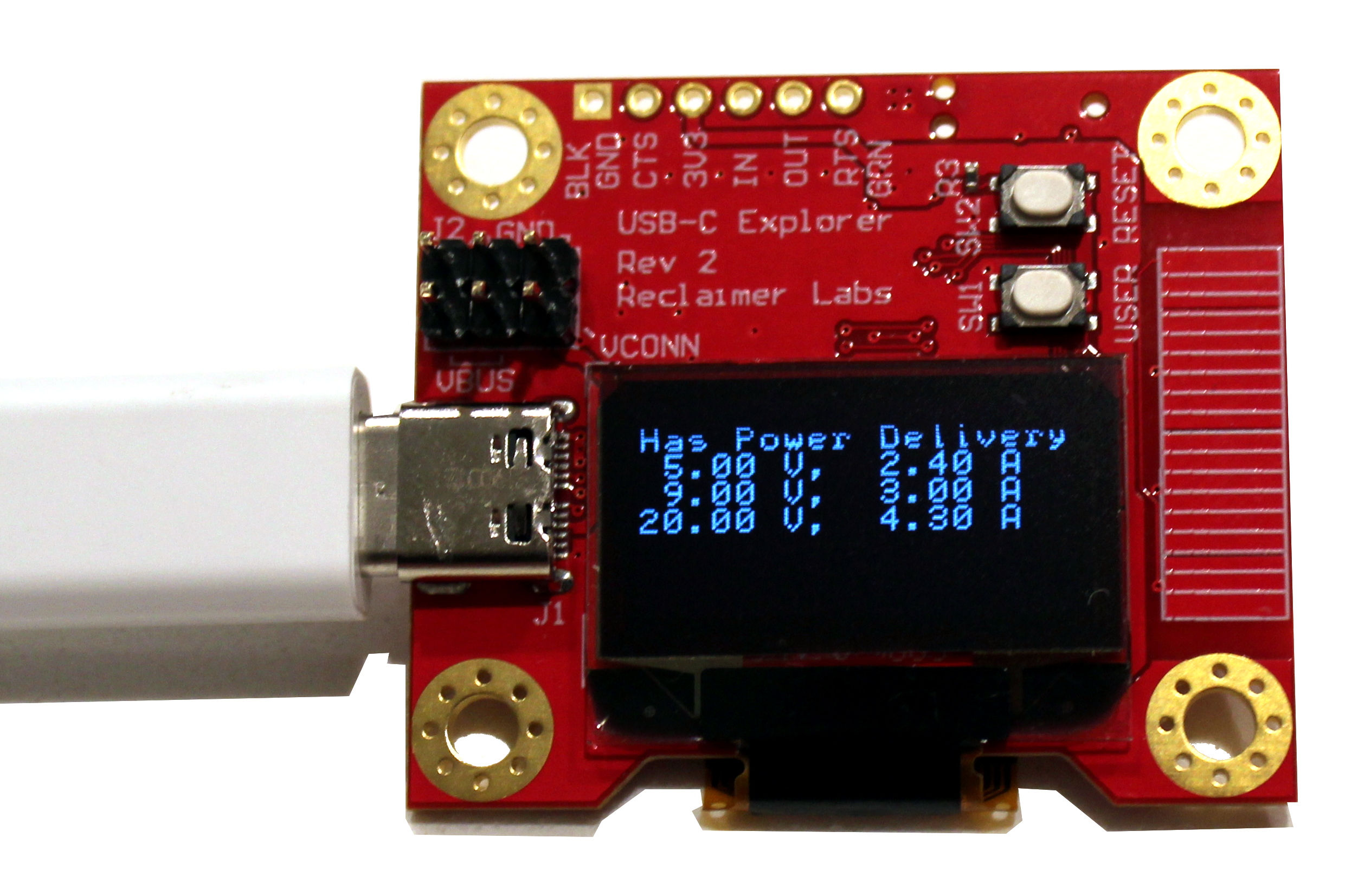
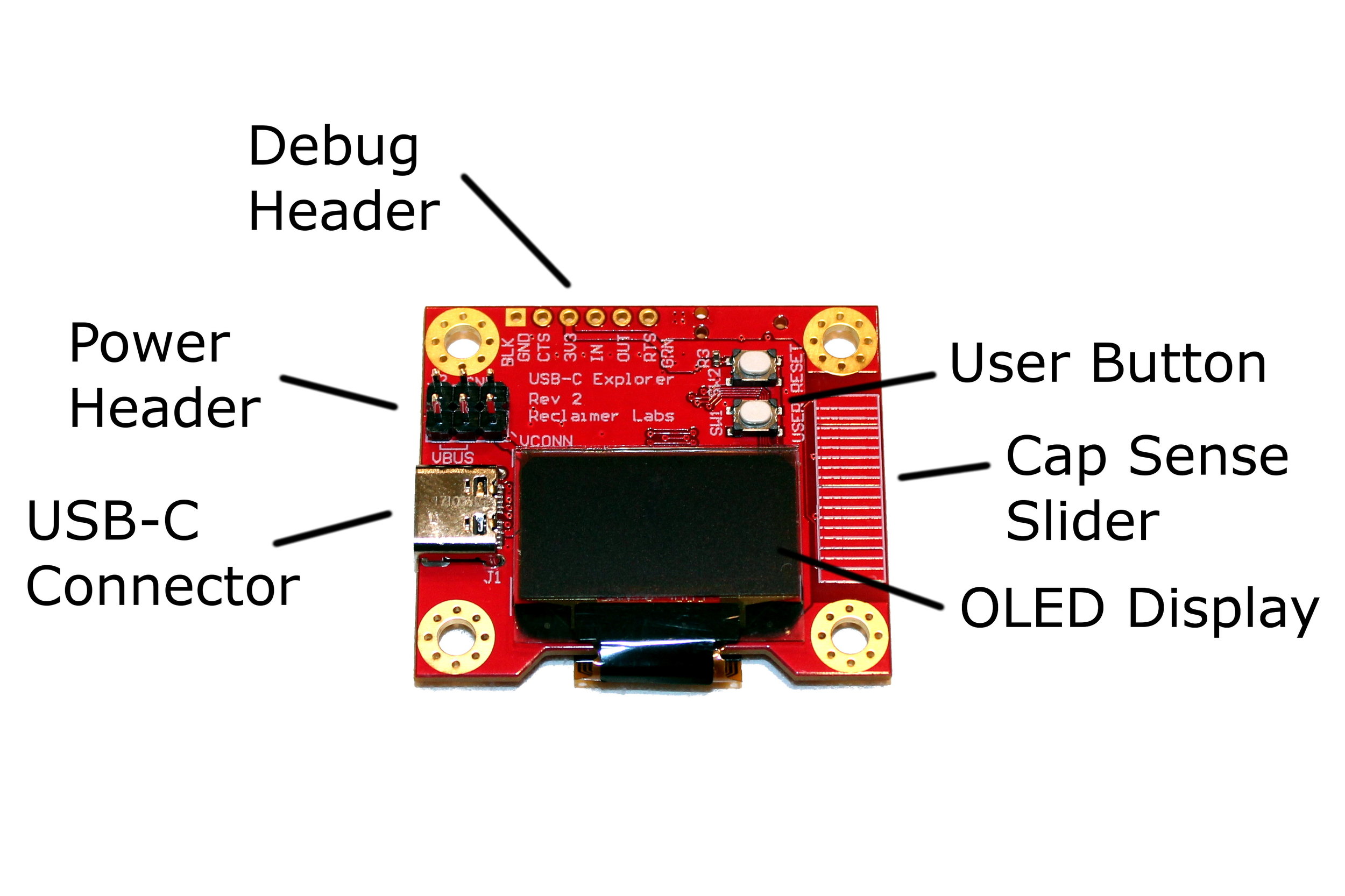
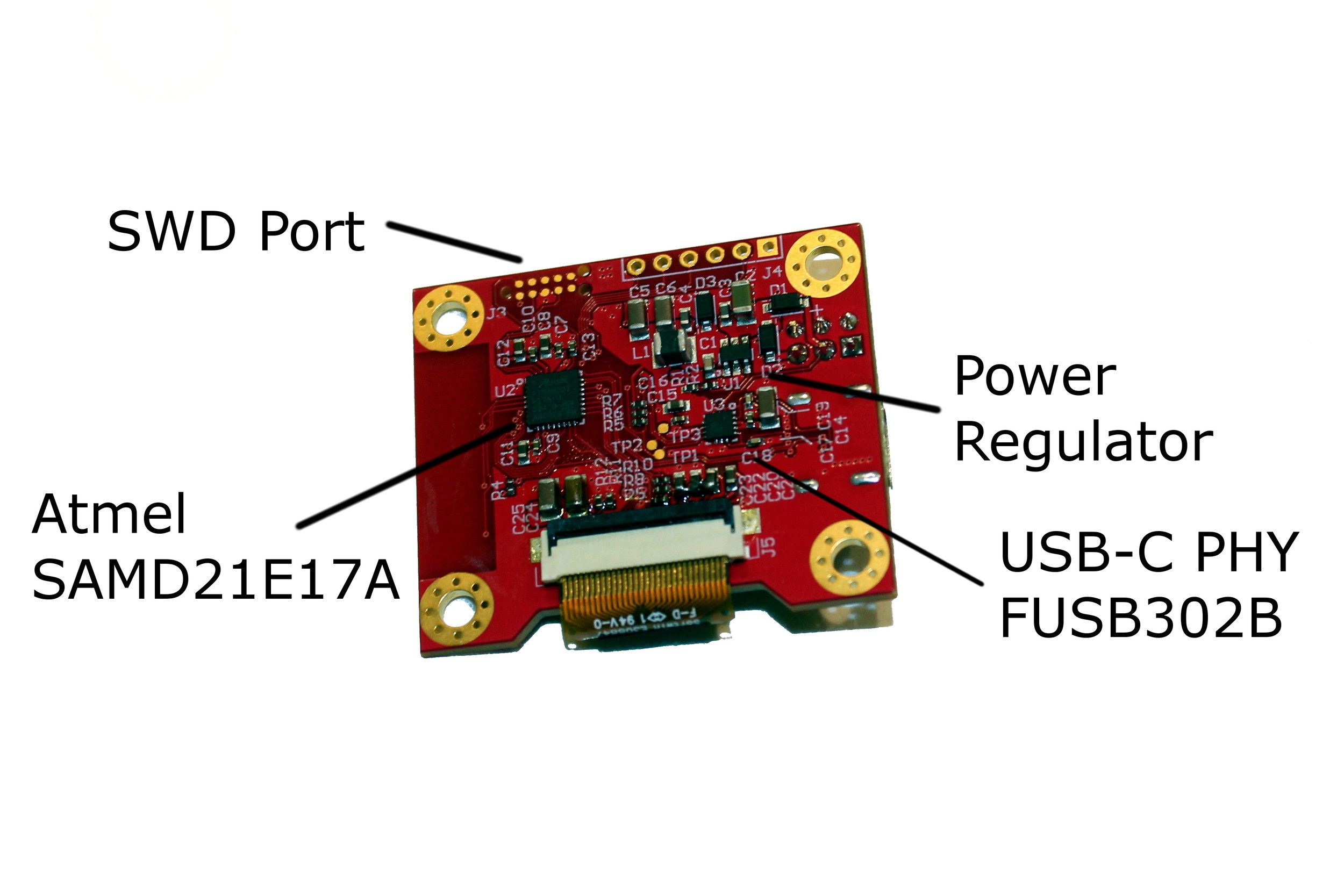
USB-C PD Breakout Board Rev 4

Final version of the test fixture
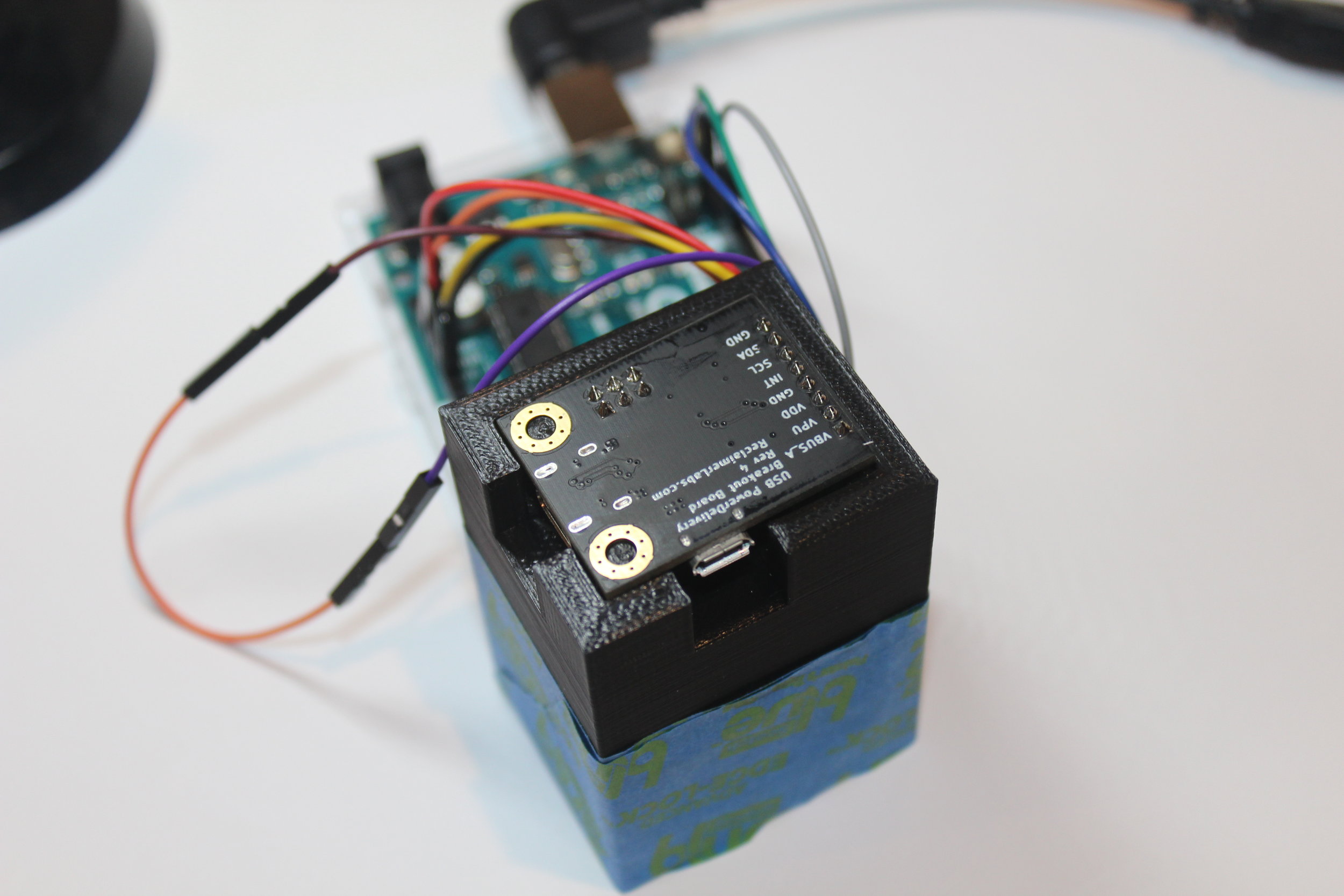
Test fixture with PCBA ready
Initially I considered some other options. I could buy a basic fixture from Aliexpress or similar sites. Those tended to be hundreds of dollars (USD). Then I would still have to fabricate custom plates for top and bottom, probably best done with a laser cutter or CNC router and a kit of pogo pins and spacers. Another option I found was OpenFixture by Tinylabs. It uses OpenSCAD to programmatically generate a box that can be laser cut. Neither of these options were good for me, as I do not have a laser cutter in my lab (yet). However, I do have a 3D printer (on loan from a friend).
My plan to 3D print the fixture worked out well, though it took a few tries. I used OnShape to capture the mechanical design. Here is a direct link to my design. All my testpoints were on the same side of the PCB, which is pretty much the only way this approach will work. The basic idea was to first create a box, then cut out clearances for the components and such, then add drill holes for the pogo pins. There are four levels of cut-outs. The first was for the really tall headers, second for the USB connectors and their cables, and third for the rest of the SMT components. The fourth level was for the actual board. I added a ring around each mounting hole and two tabs on the back side, which has no mounting holes. This level also leaves behind pins that go inside the mounting holes and the pocket for the outline of the PCB. I also had to consider the height of the pogo pins to make sure they didn’t stick up too high. There are two problems with them being too proud. First is that it take a lot more force to compress the board all the way down to the fixture. Another more serious concern is that you could short something out on your way down. I set my pogo pins to stand about 1 mm below the upper level of the fixture so the board is aligned before it makes contact. Then it has another 1 mm or so until it bottoms out, which is plenty of spring travel to make a good connection.
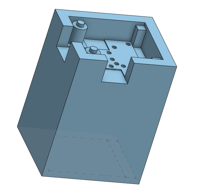
Final CAD form
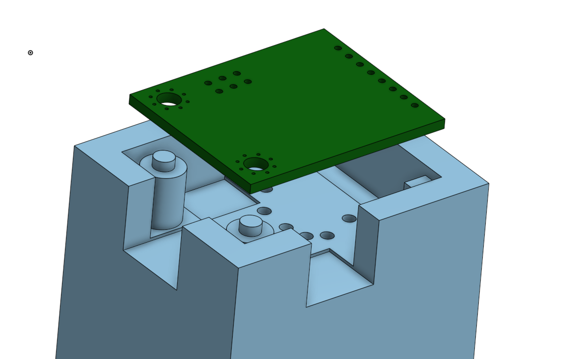
Final CAD with PCBA step file imported for fit check
Here are some technical notes on using 3D printing for PCBA test fixtures. I’m using the LulzBot TAZ 6 with 3mm black PLA from eSUN. It’s an FDM type 3D printer, which has certain limitations, especially with small, precision detail. I found that the holes it made were undersized and the pins were oversized. I wanted a 3.5 mm (+0/-0.1) pin for the mounting hole, but I had to set it to 3.2 mm in the CAD. For the holes for the pogo pins, I had to set the hole size to 2 mm to get something like 1.5 mm. At first I thought I’d have to drill the holes out after printing, but those numbers create a snug fit on their own. If you go this route, I encourage you to consider starting with a test print to get the settings right for your particular setup.
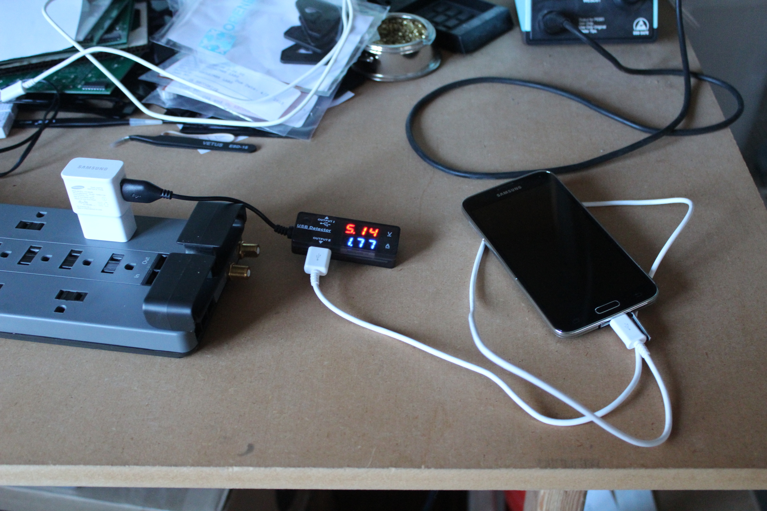
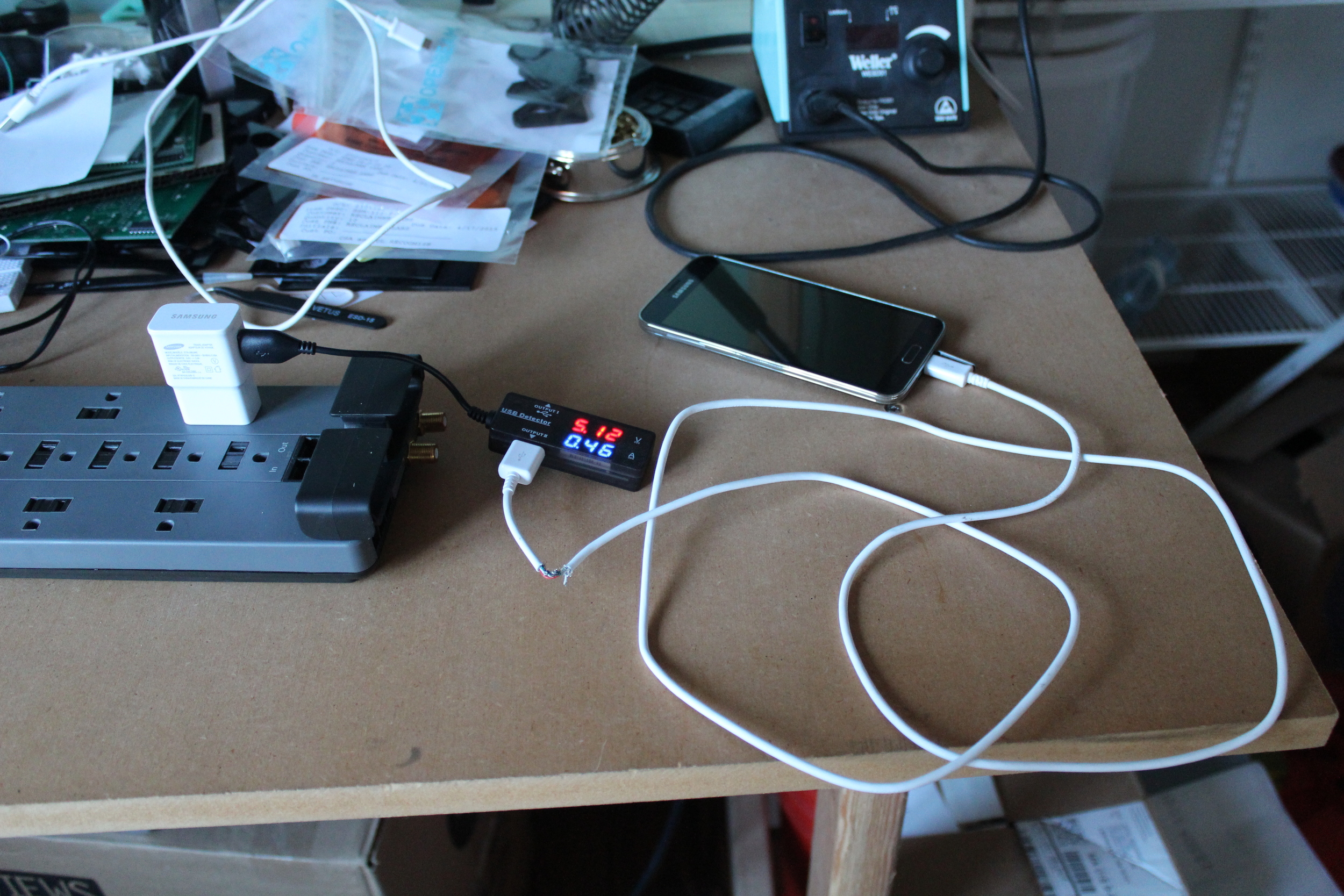
The pogo pins I used are from Dangerous Prototypes. They don’t make too many guarantees on their quality, but they worked just fine for me. I used the R100-4S sockets and the PA100-J1 pins. I didn’t feel the need to glue them in, but it’s certainly an option to make the fixture more robust, at the cost of making it less serviceable. I tinned each solder cup, then soldered pre-tinned jumper wire leads to connect each testpoint. Everything gets routed to an Arduino. For future designs, I’d recommend making sure you have plenty of space to get a soldering iron in there. It was a little tight this time, and I almost burned my fingers. Another option is to get pogo pins with a connector of some on the back, maybe something that can take a standard female 0.1 inch pre-formed jumper.
3D printing a PCBA test fixture is definitely a viable option, though there are some limitations with the way I did it. It only works if all testpoints are on one side of the PCB, unless you design a top and a hinge. I also have a minimum spacing of 2 mm center-to-center for testpoint placement, although your printer and pogo pins might allow tighter packing. Finally, the PLA material has some limitations. It’s lightweight, which allows the fixture to fly across the table if you’re not careful. Additionally, it doesn’t do well in warm, wet environments, and might degrade long term. If the benefits of being able to print your fixture in a couple hours outweigh these limitation, it’s a great option. Let me know what you think in the comments.